Entangled quantums and perfect crystals
Two Adlershof-based researchers are being granted 1.5 million each by the European Research Council
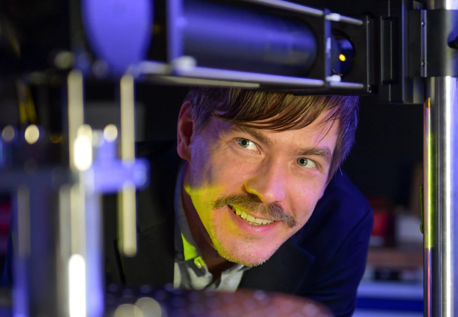
What Tim Schröder and his team are doing is essentially staging a relay race between light particles, which, upon reaching the finish line, transmit a message composed of different quantum states. These messages are known only to the sender, readable only by the recipient, and indecipherable even by the most cunning of hackers. The photons, i.e., the particles conveying the information, need a fresh up several times on the way.
This is essentially what so-called quantum repeaters do that are built into optical fibres. ‘Without them, any information would just get lost after about 100 kilometres,’ says Schröder, who is a researcher at Humboldt-Universität zu Berlin (HU) and head of a working group at the Adlershof-based Ferdinand-Braun-Institut (FBH). The physicist, who did stint at MIT after completing a PhD at HU, recently secured an European Research Council (ERC) early-career starting grant for the project QUREP (Quantum Repeater Architectures Basedon Quantum Memories and Photonic Encoding). His contribution to developing a quantum internet is funded by the ERC with 1.5 million euros for a period of five years.
The project is built on quantum bits. While conventional bits can only switch between zero and one, on and off, quantum bits can superimpose many variations of zero and one on each other. A quantum bit is realised by photons and the entanglement of photons with each other. This connection is inextricable regardless of the distance between them. These properties are used to create perfect cryptography systems because any illicit log-in will be registered immediately.
For the quantum internet to function at a global level, a drastic increase in the reach and number of photons is required. This is what the teams of HU and FBH are working on. ‘We are developing a new type of quantum repeater,’ says Schröder. They are doing this by combining novel quantum storage in diamond with indium gallium arsenide (InGaN)-based quantum emitters and integrating them into the optical fibres. The thus produced photons are capable of transmitting quantum information over thousands of kilometres while retaining a high transmission rate – think back to the relay race image from the beginning!
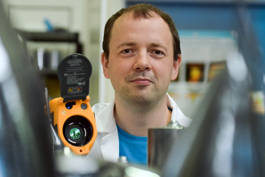
However, the building blocks of microelectronics can only operate seamlessly if they have a perfect crystal structure. This is where the experts of the Leibniz-Institute for Crystal Growth (IKZ) from Adlershof come into the picture. One of these experts is Kaspars Dadzis. After studying at the University of Latvia in Riga and earning his PhD at the Freiberg University of Mining and Technology, he is now the IKZ’s first early-career scientist to receive an ERC starting grant for the project Next Generation Multiphysical Models for Crystal Growth Processes (NEMOCRYS). The physicist is working on optimising the growth process of silicon crystals using numerical simulation.
‘A fundamental problem is that parameters such as the temperature distribution during melting, or the flow patterns during the growth process are very difficult and sometimes almost possible to measure,’ says Dadzis, who also has past experience in applied industrial research. The large, vacuum-sealed machines operate at temperatures beyond 1,400 degrees and are very hard to access. Because of this, it is only possible to estimate the effects of changes in parameters like pressure or temperature and to roughly simulate the growth process. Optimising the process would require better data. ‘Overall, the melting of silicon is very similar to melting metals,’ says the head of the IKZ working group ‘Model Experiments.’ Using materials with a low melting point could facilitate gleaning robust experimental data for validating numerical simulations. Gallium, which melts at 30 degrees, or tin, with a melting point of 230 degrees, could serve as a model substance that is much easier to work with. ‘The physics of it is in many ways similar to silicon,’ explains Dadzis.
During his project, Dadzis also strives to set up a comprehensive model experiment for crystal growth. By using sensors in a machine of his own design to measure five variables, including thermal fields, fluid flows, stress distributions, melt flow, and gas flow, he is bent on capturing ‘the entire physics of crystal growth.’ This includes particularly tricky issues like the surface tension of growing crystals that can lead to them bursting. Dadzis’ method for numerical simulation could prevent this from happening in the future.
By Paul Janositz for Adlershof Journal

