HZB patent for semiconductor characterisation goes into serial production
Newly developed monochromator determines optoelectronic and optical properties of semiconductor materials
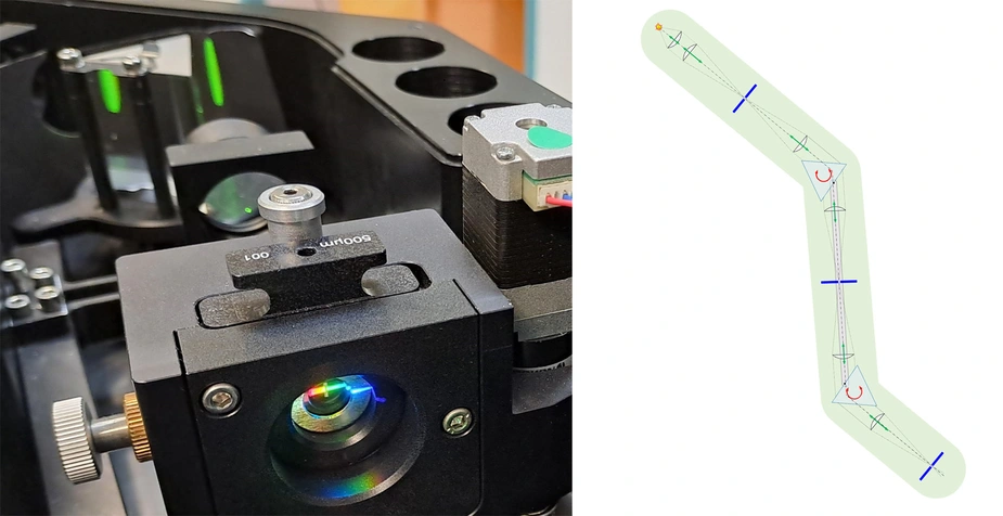
An HZB team has developed together with Freiberg Instruments an innovative monochromator that is now being produced and marketed. The device makes it possible to quickly and continuously measure the optoelectronic properties of semiconductor materials with high precision over a broad spectral range from the near infrared to the deep ultraviolet. Stray light is efficiently suppressed. This innovation is of interest for the development of new materials and can also be used to better control industrial processes.
Electronics, power electronics, light-emitting diodes, sensors, photocatalysis and photovoltaics - these technologies are based on semiconductors with band gaps ranging from the near infrared to the deep ultraviolet. New semiconductor materials with interesting optoelectronic properties are constantly being developed. In particular, the spectrally dependent photoelectric characterisation of semiconductor materials requires light sources whose photon energy can be continuously varied. Such light sources consist of a lamp, which emits light over a broad spectral range, and a monochromator, which filters out light in narrow spectral ranges. Until now, only diffraction grating monochromators have been used commercially, requiring up to five different diffraction gratings to cover a wide spectral range.
Mirrorless double prism monochromator
At the HZB, a team led by Dr. Thomas Dittrich, in collaboration with HEREON, has now developed a mirrorless double prism monochromator based on fused silica (quartz glass). Since fused silica is transparent in a spectral range from about 0.4 to over 7.3 eV, light can be spectrally dispersed over this range with just one fused silica prism. A first prototype was realised together with Freiberg Instruments. The novel, now patented, monochromator consists of a fused silica optics with two prisms and some lenses, where in addition to the dispersion-dependent rotation of the prisms, a precise adjustment of the lenses is done via stepper motors. A laser-driven xenon lamp provides high light intensities even in the deep ultraviolet.
Fast characterisation
The new monochromator makes it possible to determine the optoelectronic and optical properties of semiconductor materials in a single continuous measurement over a very wide spectral range from the near infrared to the deep ultraviolet. An additional advantage: stray light is suppressed very strongly (by more than eight orders of magnitude), which makes the monochromator particularly suitable for the photoelectric characterisation of defects in semiconductors. Due to its high intensity even in the deep ultraviolet, the monochromator is also excellently suited for the characterisation of semiconductor materials with wide or ultra-wide band gaps, such as silicon carbide and gallium oxide for high-performance electronics, diamond for IT technologies and gallium nitride for optoelectronics. With the new compact monochromator, for example, it is now possible for the first time to characterise defect states across almost the entire band gap of aluminium nitride in just a few minutes.
Applications in research and industrial production
The new monochromator improves the characterisation of electronic properties, especially of wide and ultra-wide bandgap semiconductors. This innovation is therefore not only relevant for the research and development of new materials, but can also be used in process development and industrial process control. In collaboration with Freiberg Instruments, the HZB researchers have already built a prototype and presented it in the journal Applied Optics and at conferences. Freiberg Instruments is introducing this compact monochromator into the market now. “There is a lot of interest and demand,” says Thomas Dittrich.
Publication:
Applied Optics (2024): Mirrorless fused silica based double-prism monochromator for continuous measurements from the near infrared to deep ultraviolet
Thomas Dittrich, Steffen Fengler, and Michael Franke
DOI: 10.1364/AO.529366
Contact:
Helmholtz-Zentrum Berlin für Materialien und Energie
Dr. Thomas Dittrich
Young Investigator Group Nanoscale Solid-Liquid Interfaces
+49 30 8062-17168
Email
Dr. Antonia Rötger
Press Officer
+49 30 8062-43733
Email
Press release HZB, 10 October 2024
