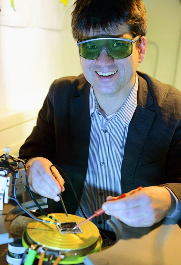
New recipes from the silicon kitchen
Research projects of Helmholtz Institute Silicon Photovoltaics
No superlative seems to be too small for the miracle material graphene. Its discovery has even reaped a Nobel Prize, the European Union has ploughed billions of euros into its research, and this ultra thin and robust material of carbon atoms is already being acclaimed the “silicon of the 21st century”. It comes as no surprise, therefore, that silicon specialists in Adlershof are examining its potential in solar cells.
Graphene is a two-dimensional honeycomb structure of carbon atoms and is an excellent conductor. Two researchers at the Institute Silicon Photovoltaics of Helmholtz-Zentrum Berlin (HZB) recently published spectacular findings: graphene also retains its outstanding electrical properties when it is heated to several hundred degrees and is coated with a thin layer of amorphous or polycrystalline silicon. The electrical conductivity in the embedded grapheme layer is thirty times higher than in contacts of zinc oxide.
Yet graphene is only a new material that the researchers at the Institute Silicon Photovoltaics are combining with the most commonly used material for solar cells. “We’re also working on hybrid concepts of organic and inorganic substances and experimenting with the mineral perovskite,” reported the Head of Institute Professor Bernd Rech. Organic polymer constituents and perovskite are easy to obtain and could make solar modules even cheaper than before.
The Institute’s second major research field deals with thin film cells of amorphous, i.e. noncrystalline silicon. “Our prime target is to apply a thin coat of silicon on glass substrates,” explained Rech. To this end, the HZB researchers apply a method for crystallising liquid glass by means of lasers. A third main field of research treats the analysis of materials. In order to analyse the properties of new cell materials even faster, the scientists will be putting into operation the new laboratory EMIL (Energy Materials In-situ Laboratory Berlin) in 2014. Covering 1000 square metres, the laboratory building will take the form of a new annexe to the BESSY II storage ring operated by the Helmholtz-Zentrum Berlin.
The Institute Silicon Photovoltaics is striking the bridge to industry via the HZB technology transfer centre PVcomB. The production line there, an own development, can manufacture silicon thin film modules. Together with two industrial partners, the Institute is currently preparing the disincorporation of a new thin film company in the Adlershof Technology Park.
By Manuel Berkel for Adlershof Special
