Solar cells: Losses made visible on the nanoscale
Researchers from HZB and University of Utah, USA, have shown how contact layers of silicon solar cells generate loss currents and what their physical origin is
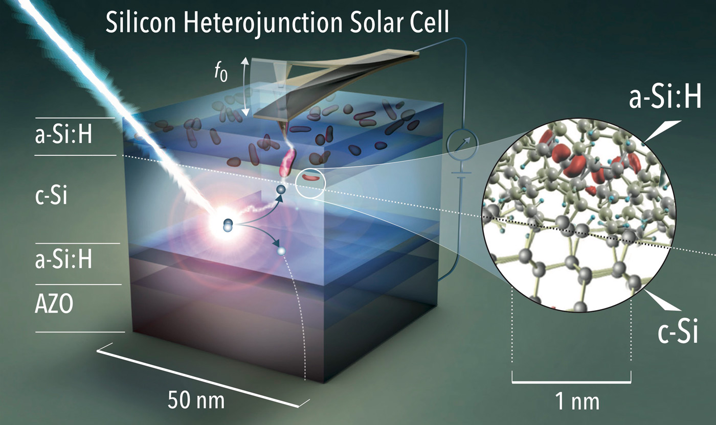
Solar cells made of crystalline silicon achieve peak efficiencies, especially in combination with selective contacts made of amorphous silicon (a-Si:H). However, their efficiency is limited by losses in these contact layers. Now, for the first time, a team at Helmholtz-Zentrum Berlin (HZB) and the University of Utah, USA, has experimentally shown how such contact layers generate loss currents on the nanometre scale and what their physical origin is. Using a conductive atomic force microscope, they scanned the solar cell surfaces in ultra-high vacuum and detected tiny, nanometre-sized channels for the detrimental dark currents, which are due to disorder in the a-Si:H layer.
Silicon solar cells are now so cheap and efficient that they can generate electricity at prices of less than 2 cent/kWh. The most efficient silicon solar cells today are made with less than 10 nanometres thin selective amorphous silicon (a-Si:H) contact layers, which are responsible for separating the light-generated charges . Efficiencies of over 24% are achieved at HZB with such silicon heterojunction solar cells and are also part of a tandem solar cell that lead to a recently reported efficiency record of 29.15 % (A. Al-Ashouri, et al. Science 370, (2020)). The current world record from Japan for a single junction silicon solar cell is also based on this heterocontact (26.6%: K. Yoshikawa, et al. Nature Energy 2, (2017)).
There is still considerable efficiency potential related to such heterocontact systems, however, it is not yet understood in detail how these layers enable charge carrier separation and what their nanoscopic loss mechanisms are. The a-Si:H contact layers are characterised by their intrinsic disorder, which on the one hand enables excellent coating of the silicon surface and thus minimises the number of interfacial defects, but on the other hand also has a small disadvantage: it can lead to local recombination currents and to the formation of transport barriers.
For the first time, a team at HZB and the University of Utah has experimentally measured on an atomic level how such leakage currents form between c-Si and a-Si:H, and how they influence the solar cell performance. In a joint effort, a team led by Prof. Christoph Boehme at the University of Utah, and by Prof. Dr. Klaus Lips at HZB, they were able to resolve the loss mechanism at the interface of the above mentioned silicon heterocontact on the nanometre scale using ultrahigh vacuum conductive atomic force microscopy (cAFM).
The physicists were able to determine with near atomic resolution where the leakage current penetrates the selective a-Si:H contact and creates a loss process in the solar cell. In cAFM these loss currents appear as nanometre-sized current channels and are the fingerprint of defects associated with the disorder of the amorphous silicon network. “These defects act as stepping stones for charges to penetrate the selective contact and induce recombination, we refer to this" as trap-assisted quantum mechanical tunnelling”, explains Lips. “This is the first time that such states have been made visible in a-Si:H and that we were able to unravel the loss mechanism under working conditions of the a solar cell of highest quality," the physicist reports enthusiastically.
The Utah/Berlin team was also able to showed that the channelled dark current fluctuates stochastically over time. The results indicate that a short-term current blockade is present, which is caused by local charge that is trapped in neighbouring defects which changes the energetic positioning of the tunnelling states (stepping stones). This trapped charge can also cause the local photovoltage at a current channel to rise to above 1V, which is far above what one would be able to use with a macroscopic contact. "At this transition from the nano to the macro worldwe find the exciting physics of heterojunctions and the key on how to further improve the efficiency of silicon solar cells in an even more targeted way," says Prof. Dr. Bernd Stannowski, who is responsible for the development of industrial silicon heterojunction solar cells at HZB.
Publication
Imaging of Bandtail States in Silicon Heterojunction Solar Cells: Nanoscopic Current Effects on Photovoltaics
Mandefro Y. Teferi, Hans Malissa, Anna Belen Morales-Vilches, Cham T. Trinh, Lars Korte, Bernd Stannowski, Clayton C. Williams, Christoph Boehme, and Klaus Lips
ACS Applied Nano Materials (2021). DOI: 10.1021/acsanm.0c02704
Contact:
Helmholtz-Zentrum Berlin für Materialien und Energie
Prof. Dr. Klaus Lips
Department Spins in Energy Conversion and Quantum Information Science
Phone: +49 30 8062-14960
Email: lips(at)helmholtz-berlin.de
Press Officer:
Dr. Antonia Rötger
Phone: +49 30 8062-43733
Email: antonia.roetger(at)helmholtz-berlin.de
Press release HZB, 17 March 2021