Watching indium phosphide at work
Research team from HZB, TU Ilmenau and Paderborn University gained insights into the electron dynamics in the surface of the semiconductor
Indium phosphide is a versatile semiconductor. The material can be used for solar cells, for hydrogen production and even for quantum computers – and with record-breaking efficiency. However, little research has been conducted into what happens on its surface. Researchers have now closed this gap and used ultra-fast lasers to scrutinise the dynamics of the electrons in the material.
"We are studying indium phosphide and looking at the processes on the surface of this semiconductor," says Jonathan Diederich, who has driven the joint project of HZB, TU Ilmenau and the University of Paderborn as part of a DFG package proposal for his dissertation at HZB. "Because the uppermost nanometres of the material are extremely important for the interesting processes." This is where, for example, water can be split into its components and thus supply green hydrogen. This electrophotochemical process works as follows: If a light particle hits an electron in the semiconductor, it receives energy, can leave its original place and initiates the chemical reaction. This happens via various energetic states that occur at extremely short intervals. The scientists led by HZB physicist and project manager Dr. Dennis Friedrich have now discovered nine of these states and determined their duration.
Special attention was paid to the incoming energy. Because if it is too high, a so-called hot electron is generated. The excess energy diffuses into the surrounding material and no longer contributes to hydrogen production. "If these hot electrons could be utilised, it would not only be possible to overcome the fundamental efficiency limit of photoelectrochemical applications but also that of solar cells. Because they are also subject to this limit," explains Jonathan Diederich. However, a good understanding of the electron dynamics on the surface of the material is important for this.
Semiconductors bombarded with UV laser
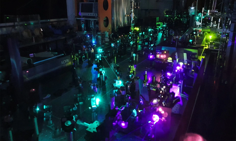
The HZB research team scrutinised these with a titanium-sapphire laser, whose beam they split. They used the first beam to nudge the electrons in the material. With the second (UV) laser beam, they imparted additional energy to the electrons and emitted them. This allowed the electrons to be measured in so-called excited states instead of resting states. "This gives us information about the permitted energetic states in these fascinating materials," says the physicist. "This is because semiconductors have a certain gap in the energy levels that electrons are allowed to occupy; this is the band gap of the material." This distinguishes them fundamentally from metals, in which electron states are possible in a continuous energy distribution. This means that electrons are not bound to an atom in the metal. They can flow and are therefore electrically conductive. The situation is completely different with insulators. There, the electrons are firmly bound; electricity is not conducted.
"In semiconductors, the electrons are released from their respective atoms above a set energy level. This leaves a gap in the energies that are permitted," adds the researcher. "Below the gap, electrons are firmly bound to the atomic nucleus, and above it, they can flow through the material." A semiconductor changes its conductivity at the "push of a button", so to speak. This can be used in a variety of ways. In computer chips, for example, where conduction and non-conduction become ones and zeros and thus enable computing. In solar cells via the photoelectric effect or in photoelectrochemical water splitting, which is being researched and optimised at the Institute for Solar Fuels at HZB under Prof. Roel van de Krol.
Ultra-high vacuum for absolute purity
One of the biggest challenges for the team was to produce the surface of the samples with the required purity. "The research group led by Prof Hannappel at TU Ilmenau took on this task," says Jonathan Diederich. "With their extensive experience in organometallic vapour deposition, they are the ideal project partner for this task."
As even the smallest impurities would alter the surface properties, everything took place in an ultra-high vacuum. This led to the second challenge. The samples had to be transported from Ilmenau to the HZB in Berlin. "To do this, we connected a vacuum chamber to two car batteries," explains the physicist. "The battery lasts four hours. If you don't make it in that time, the sample is unusable."
The measurement itself was also challenging. Time-resolved two-photon photoemission spectroscopy - as the method with the split laser is called - is a complex method, and the researchers also had to specially adapt their experimental setup. "To do this, we generate photons in the UV range," explains Jonathan Diederich. "Because we not only need a high time resolution, but also high photon energies to study the surface."
Publication:
Unraveling Electron Dynamics in p-type Indium Phosphide (100): A Time-Resolved Two-Photon Photoemission Study
Jonathan Diederich, Jennifer Velasquez Rojas, Mohammad Amin Zare Pour, Isaac Azahel Ruiz Alvarado, Agnieszka Paszuk, Rachele Sciotto, Christian Höhn, Klaus Schwarzburg, David Ostheimer, Rainer Eichberger, Wolf Gero Schmidt, Thomas Hannappel, Roel van de Krol, and Dennis Friedrich
Journal of the American Chemical Society 2024 146 (13), 8949-8960. DOI: 10.1021/jacs.3c12487
Contact:
Helmholtz-Zentrum Berlin für Materialien und Energie (HZB)
Institute Solar Fuels
Dr. Dennis Friedrich
Project lead
+49 30 8062-42923
friedrich(at)helmholtz-berlin.de
MSci. Jonathan Diederich
Doctoral researcher
jonathan.diederich(at)helmholtz-berlin.de
Press release HZB/Kai Dürfeld, 15 May 2024
