Precision made in Berlin
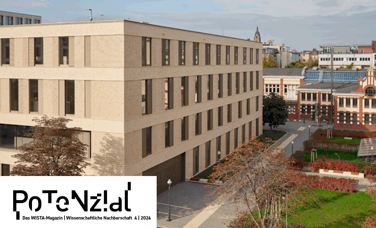
Physikalisch-Technische Bundesanstalt (PTB), Germany’s national metrology institute, is considered the cradle of quantum physics and tests the limits of what can be measured. The PTB’s Institut Berlin, or IB, is based in a thriving neighbourhood in Charlottenburg.
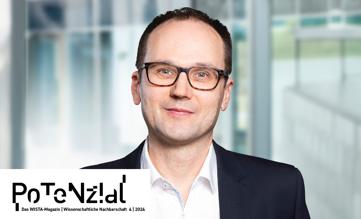
Whenever something requires high precision, the PTB comes into play. As the national metrology institute, it is also the highest authority in Germany for all issues related to correct and reliable measurements. “Objectivity, passion, and precision—that’s what PTB stands for,” explains Tobias Schäffter, head of Institut Berlin (IB) in Charlottenburg.
A place steeped in history. In 1887, when Charlottenburg was still outside of the city gates, the industrialist Werner von Siemens laid its foundation stone out on a greenfield site. Von Siemens aimed at creating a place to promote quality assurance and standardisation for the newly emerging electrical industry. This had many reasons, not least that the designation of origin “made in Germany”, which the British had introduced as protection against supposedly inferior, imported German goods, was a thorn in his eye. The rest is history.
In the same way that “made in Germany” has long become a sought-after seal of quality worldwide, the PTB has become the foremost authority in all things regarding measurement accuracy in material science, quantum technology, medicine, and data. Two of the nine specialist departments on the science of measurement (metrology) are housed at the institute’s birthplace in Charlottenburg (the headquarters emigrated to Braunschweig after the war). Around 500 researchers work in the fields of temperature and synchrotron radiation as well as medical physics and metrological information technology. In addition to the Campus Charlottenburg, the PTB uses the electron storage ring BESSY II of Helmholtz-Zentrum Berlin in Adlershof and its own Metrology Light Source (MLS).
“The IB is a thriving part of Berlin's scientific landscape due to its close proximity to Technische Universität Berlin in Charlottenburg and Humboldt-Universität zu Berlin in Adlershof as well as its diverse collaborations with non-university research partners,” says Schäffter, who appreciates and utilises these fruitful neighbourly relationships. He also appreciates and utilises a thriving network of research, industry, policy and culture—in the spirit of the salonnière Anna von Helmholtz, the wife of the first president of the institution's imperial predecessor, Hermann von Helmholtz, who also fostered this exchange.
The metrological opportunities of working with synchrotron radiation at BESSY II and MLS have proven especially fruitful for IB’s 100 employees. They conduct research and development for optical space instruments, materials metrology, and the industrial sector, among other things. An example of the latter is research on the next generation of microchips, which will power the smartphones and computers of the future. This is commissioned by companies like the Dutch ASML Holding N.V., for example, or Carl Zeiss AG. “Research must result in application. Here, too, we stand in the tradition of our founding fathers, Werner von Siemens and Hermann von Helmholtz,” says Schäffter with emphasis. And so the opportunities for collaboration found on Campus Adlershof, where research and industry go hand in hand, are highly valued.
The PTB’s new Walter Meißner Building is further proof of this. The Berlin branch of the Quantum Technology Competence Center (QTZ) features laboratory, measurement, and cleanroom spaces for high-precision temperature measurements and for research work on superconducting sensors. The Centre conducts research, development and calibration work in the field of thermometry and measurement technology that is carried out at temperatures of minus 273 degrees Celsius, close to absolute zero.
The focus here is on highly sensitive superconducting quantum interference devices, or SQUIDs—research on the cutting edge. SQUID sensors serve to measure very small magnetic fields, including brain activity in medicine or discharge processes in electric cars to improve batteries.
“We took cues from Adlershof for the Walter Meißner Building. In some ways, we sought to replicate the Technology Park on a smaller scale and make unique measurement technology available to small and medium-sized companies,” says Schäffter. This enables smaller players to test the limits of what can be measured and rapidly bring their made-in-Germany innovation to market.
Chris Löwer for POTENZIAL