Printing solar cells and organic LEDs
Humboldt-Universität zu Berlin and Helmholtz-Zentrum Berlin form a joint lab and research group “Generative production processes for hybrid components”
Solar cells, LEDs and detectors made of organic and hybrid semiconductors can nowadays be simply printed out, even together with teensy nanostructures that make them function better. The development of low-cost printing methods for electronic and optoelectronic components is at the centre of things for the new joint research group and the joint laboratory of the Helmholtz-Zentrum Berlin (HZB) and Humboldt-Universität zu Berlin (HU).
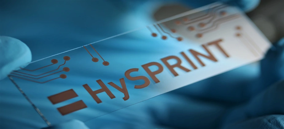
Cooperating together in the new research group are the HU workgroup “Hybrid Devices” led by Prof. Dr. Emil List-Kratochvil, the HZB young investigator group of Dr. Eva Unger, the Helmholtz Innovation Lab HySPRINT, and the Competence Centre Photovoltaics Berlin (PVcomB) directed by Prof. Dr. Rutger Schlatmann. The partners are building up a joint lab at Humboldt-Universität zu Berlin that will allow the researchers to acquire and use complementary laboratory infrastructures for various coating methods.
Prof. Emil List-Kratochvil is the head of the HU workgroup “Hybrid Devices” at IRIS Adlershof, and has been working for 15 years on developing electronic and optoelectronic hybrid components, resource-efficient deposition techniques (inkjet printing) and in-situ nanostructuring and synthetic methods. This expertise complements the aims of the HZB young investigator group led by Dr. Eva Unger. She will be developing solution-based manufacturing methods for depositing perovskite semiconductor layers onto larger surface areas for solar cells. “The new research group with List-Kratochvil is a real win for us. With his experience in printed electronic components, he is an ideal cooperation partner for us,” Unger says.
In recent months, the researcher and her team have already come much closer to her goal of developing hybrid tandem solar cells with large-surface-areas in the scope of the Helmholtz Innovation Lab HySPRINT. Now, the next step is to upscale the process in order to drive the novel solar cells towards market maturity. The Competence Centre Thin-Film- and Nanotechnology for Photovoltaics Berlin (PVcomB) is the ideal partner for the development of industrially relevant manufacturing processes. The joint research group is now striving towards building a pilot line on which to develop prototypes of hybrid components.
Contact
Prof. Dr. Emil List-Kratochvil
Humboldt-Universität zu Berlin
Tel.: +49 30 2093-7697
emil.list-kratochvil(at)hu-berlin.de
hyd.iris-adlershof.de
Dr. Eva Unger
Helmholtz-Zentrum Berlin
Young Investigator Group Leader
Young Investigator Group Hybrid Materials Formation and Scaling
Tel.: +49 30 8062-13116
eva.unger(at)helmholtz-berlin.de
