• Skip to Management
  • Skip to Main menu
  • Skip to Page content
CHIC Logo
  • WISTA
  • WISTA.Plan
  • WISTA.Service
WISTA direkt
Search
  • de
  • en
  • CHIC Logo
  • News / Events
    • Overview
    • CHIC on LinkedIn
  • Company Directory
  • Working Environments
  • WISTA
  • WISTA.Plan
  • WISTA.Service
WISTA direkt

News / Events

  • Overview
  • CHIC on LinkedIn
  • Charlottenburg
  • News / Events
22. February 2021

The perfect recipe for efficient perovskite solar cells

HZB team improved the composition of material inks for the simple and cost-effective production of solar cells

Schematic: Coating with material ink © Jinzhao Li / HZB
The liquid solution of perovskite precursor, solvent, and additive flows from a slit-shaped nozzle onto the glass substrate being conveyed below. © Jinzhao Li / HZB

A long-cherished dream of materials researchers is a solar cell that converts sunlight into electrical energy as efficiently as silicon, but that can be easily and inexpensively fabricated from abundant materials. Scientists at the Helmholtz-Zentrum Berlin have now come a step closer to achieving this. They have improved a process for vertically depositing a solution made from an inexpensive perovskite solute onto a moving substrate below. Not only have they discovered the crucial role played by one of the solvents used, but they have also taken a closer look at the aging and storage properties of the solution.

Solar cells made of crystalline silicon still account for the lion's share of roof installations and solar farms. But other technologies have long since become established as well – such as those that convert sunlight into electrical energy through use of extremely thin layers of solar-cell material deposited upon a substrate. The perovskite solar cells that Prof. Eva Unger and her team at the Helmholtz-Zentrum Berlin (HZB) are researching belong to this group. “These are the best solar cells to date that can be made using a 2D ink”, the researcher explains. “And now their efficiencies are approaching those for cells made of crystalline silicon.”
 

Developing scalable methods

Many methods have been developed and used to fabricate small test cells in the laboratory, where they can be studied and improved. But industrial-scale fabrication is still a long way off. Unger knows from her own experience: “Unfortunately, processes that are optimised for fabricating small surface areas cannot always be scaled up.” In other words: Not everything that works perfectly in the lab also necessarily works economically on the factory floor. “That's why we are taking the next step and developing scalable methods. This means our team is focussing on processes for coating larger surfaces.” At the Hybrid Silicon Perovskite Research, Integration & Novel Technologies (HySPRINT) Innovation Lab, an infrastructure for collaboration between HZB and industry, the team is concentrating on processes that have already proven their importance in industry to start with.

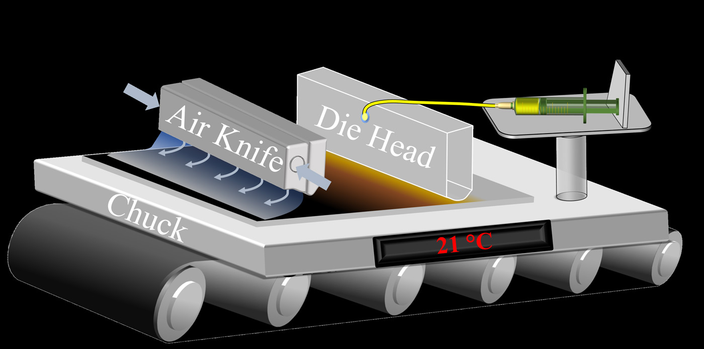
“We have experimented here with slot-die coating”, she explains. In this process, the “ink”, as the thin liquid solution of perovskite precursor, solvent, and additive is known in the trade, flows from a slit-shaped nozzle and falls like a curtain onto the glass substrate being conveyed below that will later become a solar cell. After application, crystallisation begins. An ultra-thin layer of a semiconducting perovskite structure grows that gives the material group its name and the solar cell its capabilities. Unger, together with her team members doctoral student Jinzhao Li and Dr. Janardan Dagar, have now discovered that the exact amount of an organic solvent called dimethyl sulfoxide (DMSO) in the material ink is critical for this process. Unger uses it as an additive because it has an amazing effect on the ink. “DMSO induces crystallisation nuclei for the perovskite”, says the researcher. Crystallisation nuclei usually are tiny grains that help jump-start a crystal and promote its growth. “During X-ray diffraction experiments at BESSY II, we saw quite a big difference between inks with and without DMSO added”, the physical chemist explains.
 

It's the amount that counts

However, as her team has found out in many experiments, the amount added plays a decisive role here. More DMSO favours crystal growth – up to a certain point. If this is exceeded, other processes come into play and the resulting microstructure reduces the performance of the solar cells. “It's like seasoning a soup”, says Unger. “If you add too little, it remains bland. If you add too much, it won't taste good either. So you need to add just the right amount to make it best.” In addition to the optimal composition, the HZB team has also thoroughly investigated the ageing processes and thus the storage life of the inks. “This is an aspect that has received little attention so far”, Unger explains. “The age of a perovskite precursor ink can influence device performance. This is an important factor that must be considered when developing inks and processes.”
 

Publication

20.8% Slot-Die Coated MAPbI3 Perovskite Solar Cells by Optimal DMSO-Content and Age of 2-ME Based Precursor Inks
Jinzhao Li, Janardan Dagar, Oleksandra Shargaieva, Marion A. Flatken, Hans Köbler, Markus Fenske, Christof Schultz, Bert Stegemann, Justus Just, Daniel M. Többens, Antonio Abate, Rahim Munir, and Eva Unger
Adv. Energy Materials (2021). DOI: 10.1002/aenm.202003460
 

Contact

Helmholtz-Zentrum Berlin für Materialien und Energie

Dr. Eva Unger
Young Investigator Group Hybrid Materials Formation and Scaling
Phone: +49 30 8062-41373
Email: eva.unger(at)helmholtz-berlin.de

Press Officer:
Dr. Antonia Rötger
Phone: +49 30 8062-43733
Email: antonia.roetger(at)helmholtz-berlin.de

www.helmholtz-berlin.de


Press release HZB, 22 February 2021

Research Grand Challenges Renewable Energies Microsystems / Materials

Related News

  • Visualised test scenario

    Perovskite solar cells under stress test

    Research team identifies thermal stresses as the key to long-term stability
  • BESSY II experimental hall © HZB/Kevin Fuchs

    HZB receives funding to make innovations usable more quickly

    Helmholtz Association funds innovation platforms on accelerator technologies and photovoltaics research with 4.2 million euros
  • Coatings of thin-film solar cells © HZB

    Solar cells produced from liquid inks were tested under real life conditions in the field

    HZB team optimises metal halide perovskites for the slot die coater – a step towards industrial production
  • perovskite layer model © G. Li/HZB

    Stability of perovskite solar cells reaches next milestone

    With an improved material structure, a team from HZB achieves efficiencies of up to 24.6%
  • cluster facility HZB,© B. Stannowski / HZB

    HZB cooperates with solar module manufacturer Meyer Burger

    On the way to mass production: perovskite silicon tandem cells
  • Figure: ARPES data for various photon energies © HZB

    Team at BESSY II disproves hypotheses about perovskite solar cells

    The findings enable better approaches for the targeted optimisation of this class of materials
  • Tandem solar cell HySPRINT Lab © Amran Al-Ashouri/HZB

    From Lab to Fab: World Record Solar Cell Goes from Lab to Industry

    Q CELLS and Helmholtz-Zentrum Berlin achieve record efficiency of 28.7% for 2-terminal perovskite-silicon tandem solar cell
  • Tandem solar cell © Silvia Mariotti / HZB

    Good prospects for the commercialisation of perovskite tandem solar cells

    Research teams from HZB and ISFH have combined PERC/POLO silicon cells, which are widely used on the market, with perovskite cells for the first time and estimate the efficienciy at 29.5%
  • Eva Unger © K. Kolatzki / HZB

    Humboldt-Universität zu Berlin appoints Eva Unger to professorship

    Eva Unger researches perovskite semiconductors for solar cells at Helmholtz-Zentrum Berlin and is now a professor at HU Berlin as well
  • Tag cloud Perovskite research © HZB

    A Wiki for Perovskite Solar Cell Research

    An international team of experts has designed an open source database to systematically record findings on perovskite semiconductors
  • printed spectrometer © IRIS Adlershof

    Printing an electronic rainbow

    Combination of colour printing and chemical tunability enables printed spectrometer
  • world record cell HZB. © Amran Al-Ashouri /HZB

    Another world record for HZB perovskite silicon tandem solar cells

    Almost 30 % efficiency for next-generation tandem solar cells
  • perovskite layer, HZB Adlershof Berlin, © M. Künsting/HZB

    HZB researchers provide new insights into lead-free perovskite solar cells

    How fluoride additives improve quality
  • LuQY Pro © QYB Quantum Yield Berlin

    Faster development of efficient solar cells and LEDs thanks to LuQY Pro

    HZB spin-off QYB Quantum Yield Berlin is launching a measurement instrument for optimising optoelectronic components
  • crystal structure © HZB

    New insights into the structure of organic-inorganic hybrid perovskites

    Team at HZB has analysed structural data of photovoltaic materials with a novel model
  • Samples HySPRINT-Labor © H. Näsström/HZB

    Mapping the landscape of Caesium based inorganic halide perovskites

    HZB research team studies new compositions of perovskite materials for solar energy
  • printing process © Claudia Rothkirch/HU Berlin

    First solar cells from an inkjet printer, now light-emitting diodes too

    Team of HZB and HU Berlin succeeds in inkjet printing of perovskite LED
  • 3D architecture of the cell © Burcu Kepsutlu/HZB

    “The cell looks like it has just run a marathon”

    X-ray microscopy at BESSY II reveals how nanoparticles can change cells
  • HySPRINT logo. Photo credit: Humboldt Universität zu Berlin/List-Kratochvil

    Printing solar cells and organic LEDs

    Humboldt-Universität zu Berlin and Helmholtz-Zentrum Berlin form a joint lab and research group “Generative production processes for hybrid components”
  • LinkedInshare0
  • Facebookshare0
  • WhatsAppshare0
  • E-Mail
  • © WISTA Management GmbH
  • Legal Notice
  • Privacy Policy
  • Social Media
  • Contact
Zukunftsort Charlottenburg Logo